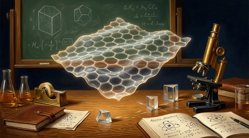
Graphene: The Carbon Monolayer and Scientific Footprints in Ecuador
Table of contents›
For much of the twentieth century, condensed matter physics accepted an almost axiomatic constraint derived from the thermodynamic foundations laid down by Rudolf Peierls and Lev Landau: a strictly two-dimensional crystal could not exist in thermodynamic equilibrium. According to the Mermin-Wagner theorem (1966), continuous symmetry breaking in spatial dimensions $d \le 2$ dictates that long-wavelength thermal fluctuations at any finite temperature ($T > 0\text{ K}$) must destabilize long-range positional order in a planar lattice, inevitably forcing the monoatomic membrane to bend, roll up, or spontaneously collapse into three-dimensional space.
Yet in the autumn of 2004, within the physics laboratories of the University of Manchester, two physicists forged in the rigorous Soviet scientific tradition challenged that consensus: Andre Geim (admired for his playful scientific curiosity, his irreverence toward dogma, and his ability to extract fundamental physics from everyday items) and his collaborator Konstantin Novoselov (admired for his experimental virtuosity, his analytical rigor, and his mastery in manipulating matter at the atomic scale). Using an astonishingly accessible laboratory procedure, they isolated for the first time atomically thin, thermodynamically stable sheets of carbon at ambient room temperature: graphene.
Formative Origins: From the Foothills of the Caucasus and the Urals to Manchester
The path leading to the isolation of graphene was not serendipitous; it was cultivated decades earlier within the unique educational climate of Soviet technical universities.
Andre Geim —in Russian, Андрей Константинович Гейм (Andrey Konstantinovich Geym)— was born in October 1958 in the Black Sea resort city of Sochi. His parents, Konstantin Alekseyevich Geim and Nina Nikolayevna Bayer, were engineers of Volga German heritage (Wolgadeutsche). Raised in Nalchik, the capital of the mountainous Kabardino-Balkar republic situated near Mount Elbrus in the North Caucasus, Geim experienced firsthand the demanding standards of Soviet provincial schooling. Despite administrative hurdles in Moscow due to his ethnic background, his perseverance enabled him to secure admission after multiple attempts to the elite Moscow Institute of Physics and Technology, known universally as Phystech (Московский физико-технический институт, Физтех), located in Dolgoprudny.
Phystech, established under the intellectual guidance of Nobel laureates Pyotr Kapitsa and Lev Landau, required students to reason from first physical principles before invoking complex formalisms. Geim earned his PhD in 1987 from the prestigious Institute of Solid State Physics of the Soviet Academy of Sciences in Chernogolovka (Черноголовка), a specialized center focused on high-purity metals and low-temperature superconductivity. Following the dissolution of the Soviet Union, Geim continued his research across institutions in Nottingham, Bath, and Radboud University Nijmegen in the Netherlands. There he developed a signature methodological tradition: the «Friday evening experiments» (Friday evening experiments), weekly sessions where he dedicated roughly $10%$ of his laboratory time and resources to testing unconventional, high-risk ideas outside officially funded research grants (an endeavor that led him, among other feats, to demonstrate the diamagnetic levitation of a live frog in 1997, earning an Ig Nobel Prize).
For his part, Konstantin Novoselov —Константин Сергеевич Новосёлов (Konstantin Sergeyevich Novoselov)— was born in August 1974 in Nizhny Tagil (Нижний Тагил), a historic heavy-metallurgy and industrial center on the eastern slopes of the Ural Mountains. The son of Sergei Viktorovich Novoselov, an engineer at the Uralvagonzavod (Уралвагонзавод) locomotive and industrial machinery works, and Tatiana Glebovna Novoselova, a teacher of English, Novoselov displayed an early talent for experimental hardware, building electrical apparatus and winning regional physics and mathematics olympiads in Sverdlovsk Oblast.
Following in Geim’s footsteps sixteen years later, Novoselov graduated with top honors from Phystech, specializing in quantum microelectronics. In 1999, Geim recruited the talented young Novoselov as a doctoral researcher at Nijmegen, and in 2001 both moved to England to join the Department of Physics and Astronomy at the University of Manchester.
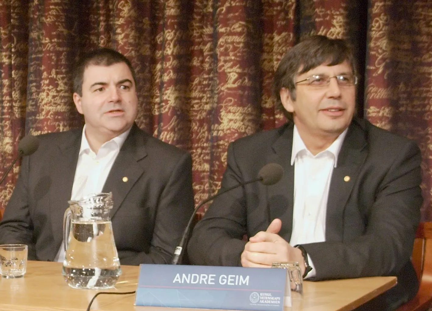 Konstantin Novoselov (left) and Andre Geim (right) during the 2010 Nobel Prize in Physics press conference at the Royal Swedish Academy of Sciences in Stockholm. Source: Wikimedia Commons / CC BY-SA 3.0.
The Breakthrough: Cleavage with Adhesive Scotch Tape
During 2004 in Manchester, Geim and Novoselov turned their attention to investigating electron transport in ultra-thin graphite films. Standard preparation protocols for scanning tunneling microscopy on graphite crystals routinely used ordinary adhesive tape to peel away outer contaminated flakes and expose pristine layers, with the tape strips habitually discarded into the wastebasket.
In one of their Friday evening sessions, the researchers chose to inspect the flaky carbonaceous residue adhering to the discarded strips of polypropylene adhesive tape (Scotch tape). Rather than throwing them away, they designed an iterative protocol of micromechanical cleavage (micromechanical cleavage): repeatedly folding and peeling the adhesive tape across the same graphite flakes to systematically divide the layers, which are held together only by weak London dispersion forces (van der Waals interactions).
Next, they pressed the exfoliated flakes onto oxidized silicon wafers coated with a thermally grown silicon dioxide ($\text{SiO}_2$) layer of precisely calibrated thickness ($300\text{ nm}$). This optical substrate was essential: while an atomic monolayer of carbon absorbs only a minute fraction of incident light, thin-film optical interference between the monolayer and the dielectric silicon dioxide substrate creates a noticeable optical contrast (between $1.5%$ and $2%$) under a standard white-light optical reflection microscope.
That milestone, published in Science in October 2004 under the title «Electric Field Effect in Atomically Thin Carbon Films», demonstrated that graphene monolayers were not only stable and reproducible at room temperature, but retained extraordinary electronic mobility—an achievement that the Royal Swedish Academy of Sciences honored with the 2010 Nobel Prize in Physics.
Quantum Physics of the Hexagonal Honeycomb Lattice
Graphene consists of carbon atoms organized in a strictly two-dimensional hexagonal honeycomb lattice (honeycomb lattice). Crystallographically, it does not form a simple Bravais lattice, but rather a triangular Bravais lattice with a two-atom basis per unit cell, conventionally designated as sublattices A and B.
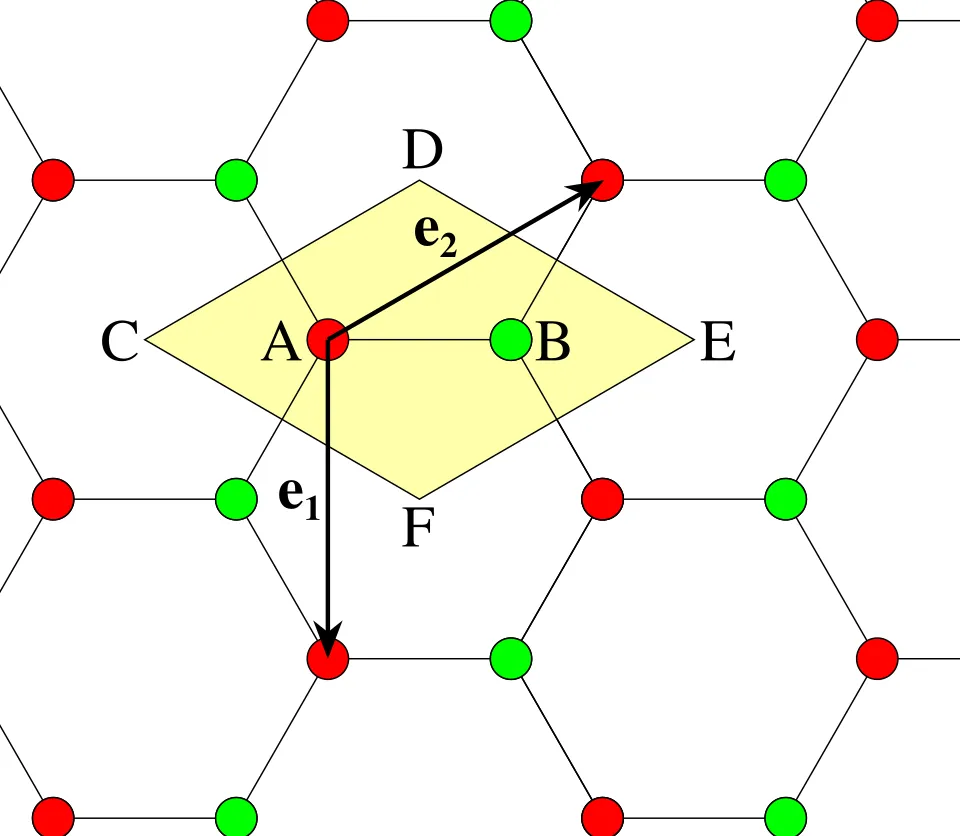 Crystallographic lattice of graphene: triangular Bravais lattice with a two-atom basis (sublattices A and B, shown in red and green), shaded rhombic primitive unit cell, and primitive translation vectors $\mathbf{e}_1$ and $\mathbf{e}_2$. Source: Wikimedia Commons / Public domain (CC0).
Each carbon atom has four valence electrons ($2s^2 2p^2$). In the plane of the sheet, the $2s$ orbital hybridizes with the $2p_x$ and $2p_y$ orbitals to form three coplanar, covalent $\sigma$ bonds through $sp^2$ hybridization, oriented at symmetric angles of $120^\circ$ with an extraordinarily short carbon-carbon bond length:
$$a_{\text{C-C}} \approx 0.142\text{ nm}$$
The fourth valence electron occupies the atomic $2p_z$ orbital, directed perpendicular to the lattice plane. Lateral overlap among neighboring $2p_z$ orbitals gives rise to delocalized bonding $\pi$ (filled at zero temperature) and antibonding $\pi^*$ (empty at zero temperature) electronic bands, which dictate charge and thermal transport.
This configuration endows graphene with remarkable physical properties:
-
Thermodynamic Stability via Microscopic Ripples (ripples):
How does graphene reconcile its existence with the Mermin-Wagner theorem? Molecular dynamics simulations and electron diffraction experiments demonstrated that the atomic sheet is not strictly planar in three dimensions: it forms spontaneous microscopic out-of-plane ripples (ripples), with characteristic amplitudes of roughly $1\text{ nm}$ and spatial wavelengths between $10$ and $25\text{ nm}$. These three-dimensional structural undulations absorb thermal excitations without rupturing the topological continuity or periodicity of the honeycomb lattice. -
Massless Relativistic Quasiparticles and Dirac Cones:
At the corners of the hexagonal first Brillouin zone, at high-symmetry points $K$ and $K’$, the $\pi$ and $\pi^*$ bands meet symmetrically at the Fermi level without opening an energy bandgap (zero-bandgap semiconductor). Near these crossing points, known as Dirac cones, the energy-momentum dispersion relation is not parabolic as in ordinary semiconductors, but strictly linear:$$E(\mathbf{k}) = \pm \hbar v_F |\mathbf{k}|$$
where $v_F$ is the Fermi velocity:
$$v_F \approx 10^6\text{ m/s} \approx \frac{c}{300}$$
As a consequence of this linear dispersion, charge carriers (electrons and holes) behave formally as massless relativistic spin-$1/2$ quasiparticles (massless Dirac fermions). Governed by the two-dimensional Dirac equation rather than the non-relativistic Schrödinger equation, they exhibit relativistic quantum electrodynamic phenomena within a solid-state material, including Klein tunneling (unit-probability transmission across sharp electrostatic potential barriers) and the anomalous quantum Hall effect observable even at room temperature.
-
Mechanical and Thermal Extremes:
Atomic force microscopy (AFM) nanoindentation measurements on suspended circular graphene membranes established a Young’s modulus of $E \approx 1.0\text{ TPa}$ and an intrinsic breaking strength of $\sigma_{\text{int}} \approx 130\text{ GPa}$, establishing it as the strongest material ever measured experimentally. Concurrently, its room-temperature thermal conductivity ranges from $3{,}000$ to $5{,}000\text{ W/(m}\cdot\text{K)}$, outperforming copper and diamond. Across the visible spectrum, its optical opacity is governed directly by quantum electrodynamics’ fine-structure constant ($\alpha \approx 1/137$): it absorbs only $\pi \alpha \approx 2.3%$ of incident white light, transmitting the remaining $97.7%$.
Graphene Research and Initiatives in Ecuador
The worldwide momentum surrounding two-dimensional materials has stimulated meaningful, tangible research initiatives across Ecuadorian academic centers, bridging sustainable agricultural waste valorization with atomic-resolution electron microscopy:
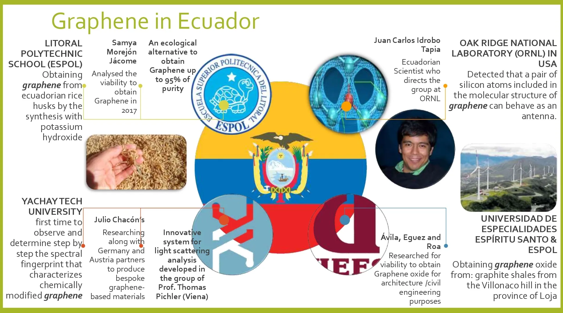 Comprehensive overview of the four pioneering graphene research fronts connected to Ecuador: green synthesis at ESPOL, atomic nanoantennas at ORNL, spectral fingerprinting at Yachay Tech, and mineral precursors in Loja (UEES & ESPOL).
1. Green Synthesis from Rice Husk Biomass (ESPOL)
At the Escuela Superior Politécnica del Litoral (ESPOL, Guayaquil), investigations developed by engineer Samya Morejón Jácome (2017) analyzed the technical feasibility of obtaining graphene as a low-cost, eco-friendly alternative from Ecuadorian rice husks (Oryza sativa), one of the most voluminous agro-industrial byproducts across the Guayas river basin. By coupling potassium hydroxide ($\text{KOH}$) chemical activation with controlled thermal pyrolysis, this agricultural waste was transformed into nanometric carbon sheets with structural purity yields reaching up to $95%$, laying the groundwork for applications in heavy-metal adsorption membranes and water desalination systems.
2. Atomic-Scale Optical Nanoantennas (ORNL)
Ecuadorian materials scientist Dr. Juan Carlos Idrobo Tapia, while directing the advanced electron microscopy group at Oak Ridge National Laboratory (ORNL, Tennessee, USA), co-led cutting-edge experiments utilizing aberration-corrected scanning transmission electron microscopy (STEM). His team discovered that an isolated pair of silicon atoms substitutionally incorporated into the molecular network of the graphene lattice can function as an atomic-scale optical nanoantenna, capable of focusing, routing, and detecting localized plasmonic excitations with sub-nanometer spatial resolution.
3. Spectral Fingerprinting and Bespoke Materials (Yachay Tech University)
At Yachay Tech University (Urcuquí, Imbabura province), the experimental group headed by Dr. Julio Chacón-Torres, in close partnership with academic collaborators in Germany and Austria —leveraging an innovative light scattering analysis system developed in the laboratory of Prof. Thomas Pichler at the University of Vienna—, succeeded for the first time in observing and resolving step-by-step the spectral fingerprint characterizing chemically modified graphene. This insight provides the analytical foundation needed for controlled functionalization and the manufacture of tailor-made graphene derivatives (bespoke graphene-based materials) for optoelectronics and chemical catalysis.
4. Mineral Graphite Outcrops from Cerro Villonaco for Civil Engineering (UEES & ESPOL)
In an inter-institutional investigation conducted by researchers Ávila, Eguez, and Roa, uniting Universidad de Especialidades Espíritu Santo (UEES) and ESPOL, the team evaluated the viability of extracting graphene oxide from native graphite shales (graphite shales) found in geological outcrops around Cerro Villonaco in Loja province. The project evaluated applications across architecture and civil engineering, demonstrating the nanomaterial’s effectiveness as a structural additive to significantly boost the compressive strength, fracture toughness, and impermeability of construction mortars and concrete.
A Bridge Between the Atom and Technology
Graphene remains an eloquent testament to the elegance of modern condensed matter physics: the demonstration that matter confined to two dimensions not only overcomes classical thermodynamic objections, but brings relativistic quantum phenomena directly onto the laboratory workbench.
From the foundational doubts of Peierls and Landau to the ingenious Scotch-tape experiments conducted by Geim and Novoselov in Manchester, and from premier international microscopy laboratories to the research groups at Yachay Tech and ESPOL, the story of two-dimensional carbon reminds us that transformative scientific discoveries do not always require colossal installations, but an observant, serene, and open-minded curiosity capable of listening to what nature reveals.
Sources and Recommended Reading
- The Nobel Prize in Physics 2010: Graphene Summary
Official summary by the Royal Swedish Academy of Sciences regarding the 2010 Nobel Prize awarded to Andre Geim and Konstantin Novoselov for groundbreaking experiments with the two-dimensional material graphene. - The Nobel Prize in Physics 2010: Scientific Background
Official scientific background detailing micromechanical cleavage, ballistic electron transport, and the quantum characteristics of the carbon honeycomb lattice. - arXiv:cond-mat/0410550 — Electric Field Effect in Atomically Thin Carbon Films (Novoselov et al., 2004)
Open-access preprint of the milestone paper published in Science (Vol. 306, pp. 666-669) that first reported the experimental isolation of graphene and its electric field effect. - arXiv:0709.1163 — The rise of graphene (Geim & Novoselov, 2007)
Open-access preprint of the seminal review article published in Nature Materials (Vol. 6, pp. 183-191) on the fundamental physics and technological horizons of graphene. - Oak Ridge National Laboratory: Advanced Microscopy & Materials
Institutional portal highlighting research in atomic-resolution transmission electron microscopy and two-dimensional nanomaterials engineering at ORNL. - ESPOL Institutional Repository
Research publications and theses from the Faculty of Mechanical Engineering and Production Sciences on rice husk valorization for carbon nanomaterials synthesis. - Yachay Tech University: School of Physical Sciences and Nanotechnology
Research registry and academic contributions in condensed matter physics, Raman spectroscopy, and materials science.